 |
||||||||||
Glossary of Terms(not in alphabetical order) |
||||||||||
|
||||||||||
Evaporation / Substrate / UHVIn surface science
and thin film science the
evaporation of material on
top
of a substrate means depositing this material on top of a carrier on
which
it can be investigated. The material to be deposited is heated (often
in
a small crucible), and its vapor condenses on top of the substrate. The
materials
to be investigated are often very reactive, so this process as well as
the
following investigations have to be carried out in a very good vacuum,
called
"ultra high vacuum" (UHV). The very complex UHV system is needed to
protect
the materials from the environment and not the other way round.
|
||||||||||
Gd / TbChemical elements
Gadolinium (Gd) and Terbium
(Tb). Group of the
Lanthanides
or Rare Earth metals. Both are of special interest because of their
magnetic
properties. Industrial use for magnetic storage media in alloys with
iron. The goal of our investigation of these metals was to demonstrate
spin polarized tunneling.
|
||||||||||
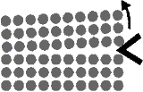
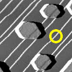
Islands / CrystallitesMaterial deposited on
top of the substrate may
cover it forming a
smooth
film or so-called "islands". These islands themselve often represent
single
crystals as well. Whether a smooth film or islands are formed
critically
depends on the properties of the substrate, the deposited material and
the
temperature. Remember water on glass: if the glass is slightly
dirty,
water forms a film on it; on fresh cleaned glass the formation of drops
is
favoured.
|
||||||||||
ReconstructionAny periodic
reorientation of the surface atoms with respect to the bulk
crystallographic structure. The motivating force may be foreign atoms
(adsorbates) or simply the fact that the atoms are at the surface (the
top
neighbours are missing). When a surface reconstructs, in most cases it
forms a -> superstructure
|
||||||||||
|
||||||||||
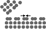
SuperstructurePeriodic arrangement
of the atoms of a deposited
material on top
of
a substrate or of the surface atoms themselves. Imagine a chessboard
with peas placed on all fields. If you
place the peas only on black fields you have arranged them in a 2 x 2
superstructure.
|
||||||||||
Single CrystalThe distinction if a
piece of stuff is amorphous,
polycrystalline or
singlecrystalline refers to the order in microscopic dimensions. The
material
itself may consist of atoms or of a chemical compound, SiO2
for
instance.
In the following schematic drawings, a square symbolizes the smallest unit of the material i.e. an atom for pure elements or a molecule for a chemical compound like SiO2.
|
||||||||||
|
||||||||||
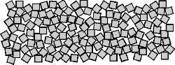
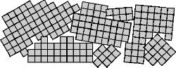
| In
an amorphous material, no long
or short
range order in between the smallest
units exists. They are bound to each other irregularely. For SiO2,
this state corresponds to its best known form: glass, with the main
component being SiO2. In a polycristalline state, a short range order exists. The material consists of many small crystallites of various size. Within the crystallites, the units are highly ordered, but no inter-crystalline order exists. Most of the materials that surround us are polycrystalline. SiO2 is found in many rocks and stones in polycrystalline form as the main component. In a single crystal, there is perfect order over the whole crystal. For SiO2, this state corresponds to rock crystal. The largest single crystals today are made for the semiconductor industry, with dimensions of several dezimeter being the topical standard. |
||||||||||
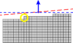
Crystallographic directionsCutting and polishing a
single crystal defines a
certain surface. The
orientation
of the surface (blue arrow) with respect to the crystallographic
structure
is given by a number in brackets.For the tungsten (W) single crystal I
used
and that is therefore the substrate for all the samples presented here
it
was the "W(110)"-direction. |
||||||||||
|
||||||||||
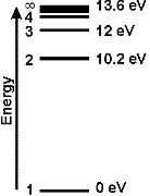
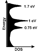
Density of States (DOS) Remember the
energetic levels of the hydrogen atom:
several distinct
states
are present. The electron that is bound to the hydrogen atom can only
persist
within one of these energetic levels. Intermediate states are
forbidden. The condensed matter energetic levels are lying so
close
together that they can not be seperated from each other. They appear to
be
smeared out to continous bands. Especially in metals there are no
forbidden
energetic levels, but the relative number of levels per energy
interval,
the density of states, may vary with energy.
|
||||||||||
|
||||||||||
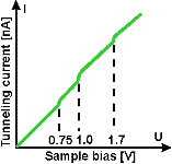
| How
will the STM
notice the condensed matter density of states? Let us take the example
DOS for a surface and look at the I-V characteristics of the tunneling
contact at a constant tip sample separation. Every
distinct state in the DOS shows up as a small
extra rise in the otherwise monotonic
rising I-V curve, located at the corresponding sample bias. The STM is
capable
of probing the sample DOS. This is the simplest form of a Scanning
Tunneling Spectroscopy, and it is in principle the way to obtain
the presented STM color images. |
||||||||||