 |
|
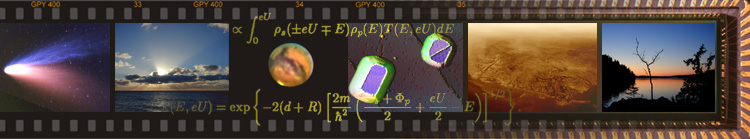
Color-Images
with the Scanning Tunneling Microscope
|
A
Scanning Tunneling Micoscope (STM) in
principle
shows the topography
of the sample being scanned, down to atomic dimensions. But this
description is only a good appoximation, in reality the
electronic structure of the sample plays an important role in the
imaging process. This fact can be used to obtain STM- images in color,
with these images not only being very aesthetical, but with the color
variations representing varying electronic structures of the sample
surface. |
|
|
|
|
|
|
Sample:
|
Surface
of a 10 monolayer thick island of Tb on W(110). The green region is the
clean Tb(0001) surface, while the blue-violet region is an adsorbate
induced reconstruction of the Tb(0001) surface. The adsorbates,
possibly CO, result from impurities from the evaporant, since the
degassing (cleaning) process of the Tb evaporation-source had not been
finished as this sample was prepared.
|
Image-size:
|
120
nm x 120 nm
|
| Image: |
topography
|
Color-information:
|
three
constant current topographical images at:
red = 0.3 V
green = 1 V
blue = 1.8 V
|
|
|
|
|
|
|
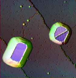
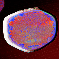
| Sample: |
Crystallites
or "islands" of GdFe2, prepared by simultanously evaporating Gd and Fe
onto the W(110) substrate and annealing at 430°C. The left island
is 2.8 nm thick. Among the islands, the substrate is covered with a
monolayer of GdFe2. The GdFe2 monolayer exhibits a slightly
different color than the GdFe2 of the islands, what means, that the
electronic structures are different. The reason is the monolayer being
stressed by the underlying W(110) substrate, with a continous stress
release to the thicker islands.
|
Image-size::
|
75
nm x 75 nm
|
Image:
|
10%
topography+ 90% deviated topography at 0.1 V
|
Color-information:
|
three
constant current topographical images at:
red = 0.1 V
green = 1 V
blue = 2.1 V
|
|
|
|
|
|
|
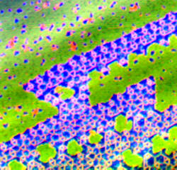
| Sample: |
About
4 monolayers of Tb on W(110), annealed at 330°C. At these
temper-parameters, the islands mainly grow along the substrate steps.
Among the islands, the substrate is covered with a monolayer of Tb. The
blue regions are hydrogen being absorbed on top of the surface.
Hydrogen is always present in small amounts in the ultra-high vacuum
chamber.
|
Image-size::
|
140
nm x 140 nm
|
Image:
|
15%
topography+ 85% deviated topography at -0.3 V |
Color-information:
|
current
imaging tunneling spectroscopy, obtained after the topography,
dI/dU images at:
red = 0.1 V
green = 1 V
blue = 2.1 V
|
|
|
|
|
|
|
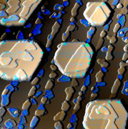
Sample::
|
About
0.3 Monolayer of Tb, less than a closed layer, have been evaporated on
top of the W(110) single crystal. The Tb atoms arrange in different,
particularely chain-like superstructures. The varying inter-chain
distance alone leads to different electronic structures of the Tb atoms
and therefore different colors of the superstructures in these
images.
|
Image-size::
|
125
nm x 125 nm
|
Image:
|
topography
|
Color-information:
|
three
constant current topographical images at:
red = 0.3 V
green = 0.8 V
blue = 1.2 V
|
|
|
|
|
|
|
Sample::
|
Island
of Tb on W(110). Again an insufficient degassing process of the
evaporant Tb leads to the colorful, but otherwise unwanted adsorbed
contamination at the rim of the island.
|
Image-size::
|
450
nm x 450 nm
|
| Image: |
10%
topography+ 90% deviated topography at 0.3 V |
Color-information:
|
three
constant current topographical images at:
red = 0.3 V
green = 1 V
blue = 1.8 V
|
|
|
|
|
|
|
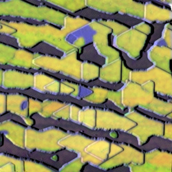
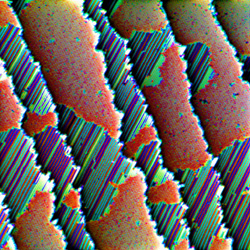
Sample::
|
Tb
terraces on W(110); during the evaporation process the substrate
temperature was lowered from 350 to 300 °C, resulting in the
formation of such step
pyramid like structures, with each step being only one single atomic
layer (0.28 nm) high. Beside hydrogen adsorbtion sites (blue) the
terraces
exhibit two kind of regions of slightly different color, yellowish and
greenish. The difference is due to stacking faults that are present in
the Tb(0001) surface.
|
Image-size::
|
200
nm x 150 nm
|
Image:
|
10%
topography+ 90% deviated topography at -0.3 V |
Color-information:
|
current
imaging tunneling spectroscopy, obtained after the topography,
dI/dU images at:
red = 0.1 V
green = 1 V
blue = 2.1 V
|
|
|
|
|
|
|
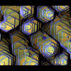
Sample::
|
Gd-
Islands on W(110). In the blue regions hydrogen has been adsorbed on
top of th Gd surface. The many small second monlayer islands seem to be
more sensitive to hydrogen adsorbtion than the thicker ones, since
hydrogen has adsorbed preferentially on them.
The reason that the color-information is dominated by the hydrogen
signal in this image lies in the very high tunneling bias of the three
color channels.
|
Image-size::
|
150
nm x 150 nm |
| Image: |
10%
topography+ 90% deviated topography at 0.3 V |
Color-information:
|
current
imaging tunneling spectroscopy, obtained after the topography,
dI/dU images at:
red = 1.2 V
green = 2.0 V
blue = 2.9 V
|
|
|
|
|
|
|
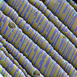
Sample::
|
Gd
and Fe have been evaporated in relation of 1:1 on top of the
W(110) single crystal, resulting in in the formation of a GdFe2 alloy,
visible as the olive-green regions. The surplus of Gd results in the
formation of the typical Gd on W(110) superstructure, visible as the
blue regions.
|
Image-size::
|
140
nm x 140 nm
|
| Image: |
topography
|
Color-information:
|
three
constant current topographical images at:
red = 0.3 V
green = 0.8 V
blue = 1.2 V
|
|
|
|
|
|
|
|
|
|
|